Determine Lead Content In Solder Alloys

For most electronics applications it is prohibited to use solders that contain lead (RoHS and WEEE directives). However, the so-called tin whiskers that sometimes grow from the surface of unleaded solder can cause short circuits – posing an unacceptable risk for high reliability (“hi-rel”) applications in aerospace and military use. To prevent this defect, a minimum lead content of 3 wt% is specified for solder used in hi-rel applications. Because the consequences of failure could be so dangerous, these specifications must be verified through measurement of the lead content.

Since the implementation of the EU directives RoHS and WEEE, lead-free solder is in common use for electronics in industrial and commercial applications. However, when exposed to stress or harsh environments (such as high humidity, vibrations, temperature variations, etc.), pure tin is susceptible to forming “whiskers” – hair-like, electrically conductive, crystalline structures of tin that grow from the metal’s surface. While tin whiskers are very thin (typically about 1 µm in diameter) their length can reach several millimetres. Numerous electronic system failures have been attributed to short circuits caused by tin whiskers that bridge closely-spaced circuit elements maintained at different electrical potentials.

Specifications for electronic components used in healthcare, aerospace and military applications therefore require a minimum of 3 wt% Pb in solder alloys to prevent the formation of tin whiskers.

Tin whiskers can cause electrical shorts between circuit Elements.

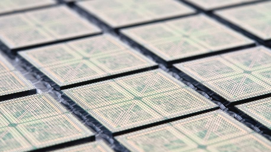
To prove that hi-rel products have been manufactured correctly, the lead content in the solder needs to be controlled and verified. A quick, reliable and non-destructive test to ensure it contains at least 3% lead or other alloying elements can be accomplished using the X-ray fluorescence method.

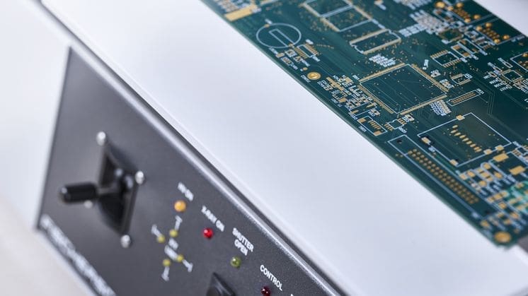
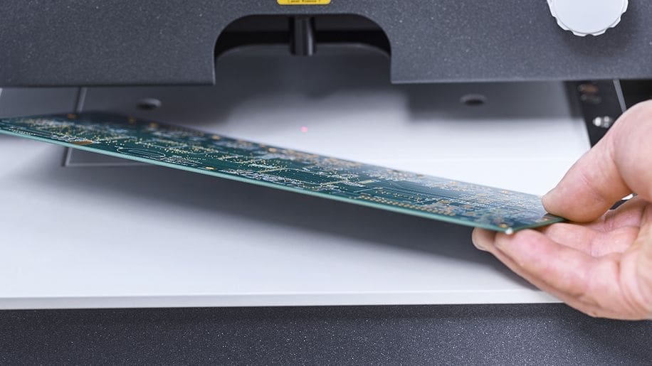
With the FISCHERSCOPE® X-RAY XDAL® it is straight-forward to measure the composition of solder alloys quickly and accurately. For example, a fast scan tells the operator if incoming parts pass inspection, eliminating the risk of mixed lots of solder. Even in rework and repair, it is indispensable for confirming the use of suitable solder. In addition, the XDAL® can be programmed for efficient screening of printed circuit boards.

The FISCHERSCOPE® X-RAY XDAL® is the ideal instrument for determining lead content in solder alloys.

The powerful software of the XDAL® simulates the entire spectrum of a defined measurement application and compares it to the spectrum actually detected, allowing accurate measurements even without calibration standards. This is especially important considering the limited shelf life of many solder alloys with lead (SnPb): In just a few years, these alloys undergo some diffusion effects (clustering of Pb) that make older standard samples often unsuitable for calibrating measurements (see Tab.1). However, FISCHER produced own SnPb standards under special manufacturing conditions to significantly reduce the aging effect.

SAMPLE AGE OF SAMPLE (YRS.) PB CONCENTRATION (WT%)
nominal XDAL Standard deviation
SnPb3 < 1 3.1 3.0 0.05
SnPb3 3-4 3.0 2.8 0.11
SnPb8 8 8.5 7.5 0.3
Eutectic SnPb > 10 38 33.6 1.0

Measurement of solder alloys of different ages are taken with the FISCHERSCOPE® X-RAY XDAL®. While a “fresh” standard is met exactly, with increasing age the deviation from nominal values increases.

With the FISCHERSCOPE® X-RAY XDAL® the lead content of electronic components can be easily checked, ensuring that enough Pb is alloyed to prevent the build-up of tin whiskers, thus avoiding potentially dangerous short circuits in high-reliability applications. For further information please contact your local FISCHER representative.

HIGHLY FLEXIBLE XRF MACHINES

Explore Further

Cover a wide range of measurement applications, such as irregular geometries and shapes, as well as big flat samples

Measure Thin Gold and Palladium Coatings on PCB Boards

As the electronics industry makes use of ever thinner coatings, manufacturers increase their demands on measuring technologies to provide reliable parameters for product monitoring. One example is the Au/Pd/Ni/Cu/printed circuit board system with coating thicknesses for Au and Pd of just a few nm. For monitoring the quality of these coating systems, X-ray fluorescence instruments have established themselves as the measurement method of choice.

The thinner the coatings, the more important it becomes to select a suitable detector. Table 1 shows a comparison of results from FISCHERSCOPE® X-RAY instruments fitted with a proportional counter tube, PIN diode and silicon drift detector (SDD), respectively.

50 nm Au 24 nm Pd
DETEKTOR TYPE Standard
deviation
Coefficient of variance Standard
deviation
Coefficient of variance
PROPORTIONA COUNTER TUBE (0,2 MM APERTURE) 2.2 nm 4.3 % 3 nm 13 %
PIN DETECTOR (1 MM APERTURE) 0.9 nm 1.8 % 1.2 nm 4.8 %
SDD DETECTOR (1 MM APERTURE) 0.2 nm 0.4 % 0.5 nm 2.1 %

Table 1. Various types of detectors and their corresponding achievable standard deviations and variation coefficients

As illustrated in Table 1 above, the SDD’s significantly superior repeatability precision allows for the reliable measurement of even very thin Au and Pd coatings.

The trueness is also better for instruments with SDD because the high energy resolution of the usable signal is less susceptible to influence from the background or adjacent fluorescence lines.

The FISCHERSCOPE® X-RAY XDV®-SDD measurement system is equipped with SDD, allowing for the quick and repeatable determination of extremely thin Coatings.

Proper handling of the fluorescence signal generated by the substrate material is also more important with thinner coatings. While a general subtraction of the background signal does improve the repeatability precision, it can also introduce errors into the results. The evaluation software WinFTM® therefore explicitly allows the composition of the substrate material to be taken into account with every measurement.

Your local contact person for FISCHER products will be happy to assist you in selecting a suitable X-ray fluorescence instrument for measuring Au/Pd coatings on printed circuit boards – FISCHERSCOPE® X-RAY XDL® with proportional counter tube, XDAL® with PIN detector, or XDV®- SDD with SDD detector.

FISCHERSCOPE® X-RAY XDL® AND XDAL®

Explore Further

Cover a wide range of measurement applications, such as irregular geometries and shapes, as well as big flat samples

FISCHERSCOPE® X-RAY XDV®-SDD

Explore Further

Precise measurements of extremely thin coatings (as low as nanometers) on complex geometry small and large samples. Ideal for PCB & ROHS

Thickness Measurement of Conformal Coatings on Printed Circuit Boards

Conformal coating material is applied to electronic circuitry to act as protection against moisture, dust, chemicals, and temperature extremes. Coatings on assemblies which are too thin or totally uncoated and therefore non-protected board parts could result in damage or malfunction of the electronics.

When electronics must withstand harsh environments and added protection is necessary, most manufacturers of circuit boards coat assemblies with a layer of transparent conformal coating. The coating material can be applied by various methods like brushing, spraying and dipping, or by selectively coating via robot. Different methods of curing/drying are available depending on the conformal coating material.

Coating thickness measurement is important to check the necessary protection level. This measurement can be performed with an eddy current method (DIN EN ISO 2360), using the copper layer as conductive background.

Special properties like the thickness of the copper layer, solder, patch size and coating type might influence the measurements. Therefore FISCHER developed a special probe type FTA3.3-5.6 HF to measure such coatings with the trueness and repeatability typical for FISCHER. For correct measuring a spot/patch size of at least 5 mm is required. Best measurement results are obtained when dedicated measuring spots are integrated into the PCB design.

Special features for the thickness measurement of conformal coatings with the probe FTA3.3-5.6 HF – connected either to FMP portable instruments or MMS PC desktop models:

  • High frequency to avoid influences caused by the variation of copper thickness
  • Large, flat probe-tip prevents indentation of soft coating types
  • Automatic conductivity compensation for base material
  • Measure on Sn, Ag or uncoated copper
  • High accuracy and repeatability

Conformal coating inspection is a critical factor in determining long term reliability of PCBs. The probe FTA3.3-5.6 HF from FISCHER is optimally suited for this application. The probe can be connected to all DUALSCOPE® or ISOSCOPE® FMP portable instruments or FISCHERSCOPE® MMS® PC desktop models.

FMP INSTRUMENTS WITH FTA3.3-5.6 HF PROBE

Explore Further

Wide range of handheld dry film thickness gauges (DFT) for the measurement of coating thickness on ferrous and non-ferrous substrates

Measure Mechanical Properties of Conformal Coatings

Determining the Quality of Two-Component Conformal Coatings on PCB with Hardness Testing

In the electronics industry, two-component conformal coatings are often used to minimize current leakage on PCBs and as protection against humidity and other environmental stressors. Because the exact composition of the polymer determines its final mechanical properties, quality control using a reliable measurement technology is mandatory.

The conformal coatings used on PCBs often consist of two components: an alcohol and an isocyanate group. For production the dosage is calculated stoichio-metrically such that a hydroxyl group of the alcohol forms a bond, or cross-link, with an isocyanate group. If there is an excess of alcohol (called “under cross-linking”), the cured polymer is not as hard and can become hygroscopic; it can also grow sticky, which causes problems further down the assembly line. If there is an excess of isocyanate (called “over cross-linking”), it can lead to reactions with humidity from the air, which generates CO2, causing bubble build-up within the lacquer.

To ensure that such problems do not develop over time, it is important to test that the composition of the conformal coating is correct. With the instrumented indentation method, the quality of the polymer can be quickly determined immediately after curing. The measurement results are not influenced by the substrate material and sample preparation is minimal. Beside the plastic and elastic deformation measurement (hardness), other parameters can also be determined, such as creep.

For technical applications the so-called “cross-link density” of the polymer is taken under consideration; Figures 2a and 2b show the results of the hardness measurement for five conformal coating polymers of different composition, as measured using the FISCHERSCOPE® HM2000. Figure 2a shows the Martens hardness over depth. The Martens hardness changes drastically depending on the cross-link density and is therefore a good indicator for the composition of the lacquer. The creep at maximum force, shown in Figure 2b, is related to the brittleness of the material and indicates an excess of isocyanate.

Martens hardness (HM) of differently cross-linked polymers;

Creep (constant force at maximum force level) as indicator for the proportion of isocyanate

Using the instrumented indentation method, the FISCHERSCOPE® HM2000 is the optimal choice to determine the quality of two-component conformal coatings on PCBs. For further information please contact your local FISCHER representative.

FISCHERSCOPE® HM2000 AND HM500 NANOINDENTERS

Explore Further

Automatic and manual stage Nanoindenters with the load range of 0-2,000mN

Measure Copper Thickness in PCB Through-Holes

As electronic devices get smaller and smaller, conducting paths must be positioned even more closely together on printed circuit boards (PCBs). This is why, today, most PCBs are multi-layered. In order to transfer electronic signals through to all the layers, these are connected by plated through-holes, also called vias (vertical interconnect access), which are electroplated with an electrically conductive material such as copper. To ensure proper function, the hole lining must be uniform.

For quality control purposes, the thickness of the copper coating lining the through-hole is measured using the eddy current method: A specially designed probe tip, housing a tiny eddy current coil, is simply inserted into the through-hole.

The coil’s special layout causes all of the eddy currents to flow longitudinally along the center line of the through-hole (Fig. 2), such that intervening copper layers exert no influence on the measurement result. Reliable measurements can even be taken despite thin layers of Sn (galvanization) on top of the plating.

Besides its ease of use, another advantage of this probe is that its range of optimum accuracy – that is, without taking any influence from the sample geometry – is for holes from 0.8 to 1.2 mm in diameter, or the typical range of PCB vias; this means that measurements can be made on multiple through-holes of different sizes without having to recalibrate in between.

FISCHER’s needle-like eddy current probe tips are made in different lengths corresponding to typical PCB thicknesses: With the ESL080B and ESL080V probes, a range of board thicknesses from 0.5 to 8 mm is covered. These probes work perfectly with FISCHER eddy-current instruments: e.g. the convenient handheld unit PHASCOPE® PMP10, or the versatile table-top device FISCHERSCOPE® MMS® PC2.

The precise measurement of copper thickness in plated PCB through-holes is made easy with specialized probes (ESL080B / ESL080V) used in conjunction with FISCHER eddy current instruments, such as the PHASCOPE® PMP10 or the FISCHERSCOPE® MMS® PC2. For additional information, please contact your local FISCHER representative.

Measure Thickness of Solder Resist on PCBs

To prevent solder from bridging conductive traces and causing short-circuits, while undergoing the soldering process printed circuit boards (PCBs) are coated with a non-conductive lacquer to which solder will not adhere. This ‘solder mask’ also safeguards the board’s circuitry against environmental influences and improves electric strength. With so much depending on this important layer, it is obvious that its quality should be monitored during manufacture.

Traditionally green in color, solder resist (often epoxide resin) was originally developed for facilitating wave soldering processes: not only to prevent unintended solder bridges but also to restrict the solder to just the electrical contacts, thereby reducing overall solder consumption. Today, even when other techniques are used, a solder resist layer is still indispensable for permanently protecting the delicate copper traces from wear, heat and moisture, as well as for insulating the PCB’s circuitry. The thickness of the solder mask is essential to its functionality and must therefore be controlled during production.

Determining the thickness of the solder resist layer implies measuring a non-conductive coating on top of copper – a clear case for using the amplitude sensitive eddy current method. Because the thickness of the covered copper layers can vary widely, one should use a high frequency probe with a low eddy current depth.

For exactly such applications, FISCHER has developed the FTA3.3-5.6HF probe. Its high frequency (20 MHz) makes a 30µm thick copper substrate sufficient to reach optimum results. If measurement uncertainties of 10-15% are acceptable, even coatings on top of copper traces only 18µm thick can be measured with this probe.

High frequency probe FTA3.3-5.6HF.

Due to the lateral expansion of the FTA3.3-5.6HF’s eddy current field, the measurement spot must be at least 5-6 mm in diameter to avoid edge effect influences on the measurement results.

To check the thickness of solder resist lacquers on PCB copper, FISCHER’s high frequency probe FTA3.3-5.6HF is ideal. The probe can be used equally well with the handheld ISOSCOPE® and DUALSCOPE® instruments of the FISCHER FMP family or with the FISCHERSCOPE® MMS® PC2 bench-top unit. Please contact your local FISCHER representative for further information.

FISCHER FMP COATING THICKNESS GAUGES

Explore Further

Wide range of handheld dry film thickness gauges (DFT) for the measurement of coating thickness on ferrous and non-ferrous substrates

Measure PCB Applications with Fischer X-Ray Fluorescence

Determining the coating thickness of standard PCB applications must be fast, precise, non-destructive and cost effective. Ever-higher volumes of standard PCBs are being produced with ever-thinner coatings, often using precious metals and requiring testing on ever-smaller structures. Plus, to be suitable for this purpose any instrument must cope with further sample handling challenges such as flexible or oversized PCBs.

The x-ray fluorescence (XRF) method has been well established for its reliability and accuracy in measuring metallic coatings on PCBs. FISCHER offers with its dedicated X-Ray PCB family an extensive array of XRF products for analyzing and determining the thickness of all the standard coatings used in practical applications on PCBs. Even complex multi-layer and (precious) alloy coating systems can be tested easily and accurately.

FISCHERSCOPE® XULM® PCB with extensions for flexible PCBs.

Various models and options address a range of needs and challenges, whether to accommodate difficult positioning requirements or small structures: the customer can choose from “top-down” or “bottom-up” instruments, manual handling or motorized XY-stages, as well as extended sample supports.

1ST LAYER 2ND LAYER 3RD LAYER 4TH LAYER
Measuring application Typical Range Typical Range Typical Range Typical Range
Au/Ni/Cu 0.3 – 0.7 3 – 15 10 – 40
Au/NiP/Cu 0.02 – 0.08 1 – 6 10 – 40
Ag/Cu 0.1 – 0.5 10 – 40
Sn/Cu 0.5 – 9 10 – 40
SnPd/Cu 2.5 – 10 10 – 30
Au/Pd/NiP/Cu 0.02 – 0.08 0.03 – 0.1 1 – 6 10 – 40

Typical PCB applications and coating thicknesses [µm].

With its focus on precision and trueness, FISCHER also provides a wide selection of calibration standards, produced in its own accredited calibration laboratory. To measure PCB layer thicknesses below 100 nm it is mandatory to calibrate the instrument with standards of similar thickness. For coatings below 50 nm FISCHER offers precise instruments with semiconductor detector.

The specially designed and developed FISCHER X-Ray PCB instruments perfectly meet the quality control needs of PCB manufacturers: Fast and easy-to-use, and equipped with matching calibration standards, they allow for highly precise, reliable and non-destructive measurements. For further information contact your local FISCHER sales representative.

Pattern Recognition to Measure PCBS

Modern printed circuit boards (PCBs) are furnished with a huge number of contact points for electrical connections, all of which are coated with metal. The metrological monitoring of these coated areas is imperative for precise process control. But especially for large-scale boards, manual positioning on these tiny measuring spots is simply unfeasible.

For the metrological monitoring of the thickness and material composition of coated contact points on PCBs, X-ray fluorescence (XRF) has been established as a very effective method. FISCHER offers several different models of its XRF systems, the FISCHERSCOPE® X-RAY series, which are specifically optimized for the measurement of contact pads on PCBs. As the demands for automation have steadily grown also for process control, the next logical step was to develop a solution for fast and effective quality control that requires minimal operator effort.

To minimize operator involvement during measurement, the WinFTM® analysis software (version 6.30 and up) now offers automatic pattern recognition. This allows accurate and precise positioning of the measuring spot on very small structures in all XRF instruments with programmable XY tables. Especially in automated processes, pattern recognition can be used effectively, for example when testing large circuit boards and measuring repeatedly at the same positions.

While is not uncommon for a small offset from the originally programmed measuring points to occur when the device is loaded with the next PCB, the true measurement position on structures in the micrometer range can only be found accurately using the fine adjustment capabilities of pattern recognition technology.

With WinFTM® , image details or patterns can be defined using the image recognition menu, which lets the user freely select the measuring position within the image frame. Then, before measuring starts, the software compares the measuring spot (in the focus of the crosshairs) with the picture detail – and automatically derives a more accurate positioning, locating and targeting the next contact pad in the row. It is also possible to define several image details or patterns in order to perform automated measurements on a variety of structures.

Using the pre-sets in the pattern recognition menu, it is easy to run this software function even without prior knowledge. In addition, a variety of search algorithms can be chosen, as well as allowing for minor deviations from the target image (pattern) via error-checking.

The new pattern recognition feature built into the WinFTM® software enables excellent automated quality control of printed circuit boards when used with the XRF measurement systems from FISCHER. For more information, please contact your local FISCHER representative.

Measure Solder Coatings on PCBs

Because EU directives like EU2002/95/EC and EU2002/96/EC prohibit lead and other heavy metals, the solderable coating systems used on printed circuit boards must now be lead free. However, immersion tin carries the risk that, due to diffusion processes, the usable tin remaining in the plating can be insufficient to guarantee the success of solder processes and the quality of solder joints. Therefore the thickness of the pure tin in the coating must be checked before soldering.

Diffusion of copper into the tin starts immediately after deposition of the tin coating. Depending on temperature and time, intermetallic compounds can form which consume the tin in the plating until there is insufficient pure tin left to produce good solder joints. The loss of pure tin is further exacerbated by the heat of the solder process itself. For proper solder joints, a minimum thickness of 0.3 µm pure tin is required before the last solder procedure, meaning an initial layer of freshly deposited tin of at least 1-1.4 µm.

FISCHER COULOSCOPE® CMS

To ensure solderability, the thickness of the remaining pure tin in the plating must be measured precisely. The Coulometric method (DIN EN ISO 2177) is the best choice for this task.

To demonstrate the diffusion problem with measurement results, PCBs with layers of ca. 0.5 and 1 μm immersion tin on top of various copper coating thicknesses were tempered and, after each heating procedure, measured with a FISCHER COULOSCOPE® CMS. The thickness of the copper coating exerted no influence on the thickness of the remaining tin.

INITIAL SN COATING THICKNESS DURATION OF TEMPERING PROCEDURE [H]
0 2 4 6
ca. 0.5 µm Mean value 0.52 0.12 0.04 (*)
Standard Deviation 0.004 0.004 0.003 (*)
ca. 1 µm Mean value 1.01 0.60 0.50 0.43
Standard deviation 0.01 0.01 0.01 0.01

Mean values in µm of 9 (0 h tempering) and 3 (2, 4, 6 h tempering) measurement series; (*) not measurable because the remaining layer of pure tin is too thin.

The jump in de-plating potential between the pure tin coating and SnCu diffusion zone.

The Coulometric method makes obvious the drop in thickness of the pure tin coating. The measurement series with the 0.5 µm samples clearly shows that, even after only two hours of tempering, too little tin remains to guarantee proper solderability.

To check the solderability of coating systems on PCBs, the thickness of the remaining pure tin can be measured without being influenced by the SnCu-alloy using the FISCHER COULOSCOPE® CMS. For more information please contact your local FISCHER representative.

Material Analysis of Solder Bumps in Integrated Circuit Packaging

Due to growing restrictions on the use of lead in electronic products, efforts have been made to find appropriate substitutes. In the advanced IC packaging industry, the formerly ubiquitous, high-quality – but hazardous – eutectic SnPb solder bumps are now gradually being replaced by lead-free technology, such as SnAgCu alloy solder bumps. Because these new alloys require a certain composition in order to assure solderability and other mechanical properties, they must be measured precisely.

It is well known that the Ag and Cu content can exert profound impacts on the solderability and mechanical properties of Sn-based solder bumps. For instance, solder bumps with Ag content of more than 3% perform better in thermal fatigue testing and are more resistant to shear plastic deformation, while alloys with lower Ag content (around 1%) exhibit superior ductility and therefore better fatigue endurance under severe strain conditions. Furthermore, a mere 0.5% of Cu can decrease the dissolution behaviour of substrate Cu, thus increasing solderability.

That is why the IC packaging industry must accurately and precisely determine the composition of solder bumps, in order to fulfil the challenging combination of legal restrictions (being lead-free) and technical requirements.

The small size of the bumps (typically 80μm in diameter) prevents the use of most analytical methods. Others, such as atomic absorption (AA), are destructive and are therefore not suitable for testing each individual bump. However, X-ray fluorescence (XRF), has proven to be an ideal approach for monitoring the concentration of all three elements. Table 1 shows typical measurement results for a SnAgCu solder bump.

FISCHER COULOSCOPE® CMS

To ensure solderability, the thickness of the remaining pure tin in the plating must be measured precisely. The Coulometric method (DIN EN ISO 2177) is the best choice for this task.

To demonstrate the diffusion problem with measurement results, PCBs with layers of ca. 0.5 and 1 μm immersion tin on top of various copper coating thicknesses were tempered and, after each heating procedure, measured with a FISCHER COULOSCOPE® CMS. The thickness of the copper coating exerted no influence on the thickness of the remaining tin.

ELEMENT SN AG CU
Mean [%] 98.55 0.99 0.46
Std.dev [%] 0.04 0.03 0.1

Typical values measured with FISCHERSCOPE® X-RAY XDV®-μ, 10 x 30sec

The X-ray beam of the FISCHERSCOPE® X-RAY XDV®-μ, equipped with poly-capillary optics and a silicon drift detector (SDD), can be focused down to measuring spot sizes as small as 20μm while still yielding very high count rates, guaranteeing outstanding repeatability and precision.

If accurately determining the composition of solder bumps – not only to verify lead-free technology – is important to you, the FISCHERSCOPE® X-RAY XDV-µ®, with its extremely small measuring spot, is the ideal instrument. For further information please contact your local FISCHER representative.